Two women in a laboratory look at a microscope.

Chemists design molecules for next-generation semiconductors

By Hannah Ashton

For decades, the semiconductor industry has followed a clear trajectory. Computers grow more powerful even as the tiny components inside microchips shrink. Known as Moore’s law — the observation that the numbers of transistors on a microchip roughly doubles every two years — this pattern has driven the development of everything from smartphones to artificial intelligence.

But what happens when engineers approach the physical limits of traditional manufacturing? Today, the patterns etched onto microchips have become so small that chemistry, not just engineering, may determine how much further computing technology can advance.

In the College of Science, materials scientist May Nyman and doctoral student Esther Julius are designing molecules that could help push those limits further.

Their research focuses on metal oxide clusters, tiny molecular structures that can act as chemical scaffolding for creating the intricate patterns used to build semiconductor chips. The work, supported in part by industry partners including Intel, is part of a broader effort by Oregon State to expand semiconductor research and strengthen ties with Oregon’s technology sector.

“We’re working at the nanometer scale, using molecules to create the patterns needed for next generation electronics,” Nyman said.

Building on a nanoscopic scale

Creating the tiny circuits that allow a semiconductor chip to process information requires a technique called lithography, essentially a way of drawing extremely small patterns that guide where materials are deposited. Nyman compares the typical pattern to a window screen with cross-hatching.

The process starts with a thin film of molecules deposited on a semiconductor wafer, using a light-sensitive material called photoresist. The wafer is then exposed to light through a mask that contains the desired pattern. The light alters the photoresist, and the pattern is etched into the wafer.

“You have channels and ordered squares, kind of like buildings and streets. Afterward, the channels or the square holes are filled in with other materials,” Nyman said. “So Esther’s work is helping to create these patterns. It’s like scaffolding.”

Layer by layer, scientists repeat this process, assembling the complex architecture that builds a microchip. The circuits inside modern chips are extraordinarily dense, with billions of transistors packed into spaces measured in nanometers.

Shrinking those features further is the next big challenge.

“We’re at the point now that the industry is making such small features that you really need to pattern them with chemistry, with molecules,” Nyman said.

Nyman’s lab is well-positioned to do this research because of its work on metal oxide clusters, molecules that contain metals bound together with oxygen atoms.

“We make molecules that contain metals because they grow beautiful crystals which are very exciting,” Nyman said. “And depending on their composition, size, properties and behavior, they can be used for different applications.”

Her group studies potential uses from carbon capture to metal separations and nuclear fuel recycling. Ph.D. student Esther Julius is leading the Intel-funded research project aimed at developing the next generation of molecules used in photoresists.

A woman in a lab coat, goggles and gloves poses for a headshot.

Ph.D. graduate student Esther Julius is exploring how metal oxide clusters can function as lithography materials used in microchip manufacturing.

Originally from Nigeria, Julius studied industrial chemistry at Kaduna State University before moving to the U.S. to attend graduate school at Oregon State.

Her research explores how metal oxide clusters can function as lithography materials used in microchip manufacturing.

“Photolithography excites me because of the way it connects fundamental chemistry with real-world applications,” Julius said. “It amazes me how the molecules we synthesize in the lab can ultimately be used as lithography materials, which are essential for microchip production.”

For Julius, this research illustrates how chemistry shapes the devices people rely on every day.

“Cellphones rely on tiny molecules and materials that work together to make the whole system work efficiently and smartly,” she said.

One of the project's goals is to make the molecules used in lithography easier to produce.

Traditional synthesis methods can require complex procedures involving specialized equipment and high temperatures. Julius has been able to simplify the process dramatically.

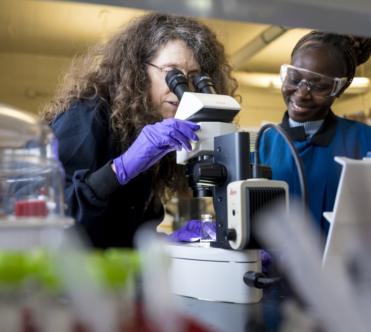
“Instead of boiling it and using a special apparatus, she mixes things in a 10-milliliter beaker, and it takes 20 minutes at room temperature,” Nyman said.

Simplifying the chemistry could make the materials easier and cheaper to manufacture if they are eventually used in semiconductor production.

“We have to rely on chemistry to do its thing.”

Working at molecular scales presents enormous scientific challenges.

“As humans, we like to control everything,” Nyman said. “As chemists, we want to control molecules.”

But chemists cannot directly manipulate individual atoms with their hands.

“We don’t have little tweezers where we can go in and say, ‘OK, I’m going to break this bond and make that bond,’” she said. “We have to rely on chemistry to do its thing.”

Small imperfections can have major consequences for semiconductor devices. Even if 98% of the molecules behave as intended, the ones that don’t create defects that are compounded into defective microelectronic circuits, Nyman said.

Designing molecules that behave reliably, even under changing environmental conditions, is a major goal for Nyman and Julius.

The pair approaches the problem from a foundation of basic chemistry.

“We’ve always been a fundamental chemistry-first lab. Understanding how molecules interact, how they behave in solution and how we can manipulate them,” Nyman said.

Applications come later. While many other researchers try to start the other way around, her lab takes a different approach.

“I call it swimming with molecules,” she said. “Picture yourself swimming among them. What are they doing?”

Two women in lab coats and gloves work inside a fume hood.

Nyman and Julius work in the laboratory with metal-oxo clusters.

The “Silicon Forest”

Nyman and Julius are part of a larger effort at Oregon State to strengthen semiconductor innovation.

“There is so much history here and discoveries and companies that were founded out of the College of Science and have connections with the semiconductor industry."

Oregon’s technology industry, sometimes referred to as the “Silicon Forest,” includes Intel’s major operations in Hillsboro, along with a network of suppliers and startups.

“There is so much history here and discoveries and companies that were founded out of the College of Science and have connections with the semiconductor industry,” Nyman said.

Those connections help create collaborations and promising career pathways for students.

“They hire our students, so they’re interested in providing training opportunities to our students,” she said.

Powering the future of computing

The demand for more powerful semiconductors continues to explode as technologies like artificial intelligence expand.

“You can’t watch or read the news on any single day now where you don’t hear about AI,” Nyman said. Advances in chemistry could help the next generation of computing hardware. “The research that we’re doing is foundational to AI. The world needs faster, better computer chips.”

For Julius, the work offers a chance to contribute to the future of technology through chemistry.

“What happens if in the future we have smarter, more efficient smartphones, computers and all electronics?” she said.

Solutions to today’s challenges may begin with molecules measured in billionths of a meter — designed in a chemistry laboratory at Oregon State.